Current-Mode Class D AM Transmitters
For 160, 75 and 40 Meters
375-Watt Carrier

375 Watt Class D

This is an update to information previously published on this website describing Current Mode Class D (CMCD) AM transmitters. That information was the result of a 'first attempt' at CMCD and a number of improvements have been incorporated since then, including the addition of a 40 meter deck. A link to the earlier and now rather dated information can be found here.

Why 'Current Mode' Class D?

Without getting too deep 'in the weeds', there are two types of Class D operation - Voltage Mode
Class D (VMCD) and Current Mode Class D (CMCD). In VMCD power to the final is derived from a voltage source and in CMCD from a current source. The drawings below illustrate the concept. Note the difference at the center tap of the output transformer - VMCD has the transformer center tap bypassed
(a voltage source) and CMCD makes use of an rf choke (a current source). The associated tank circuits also differ - VMCD uses a series tuned circuit and CMCD a parallel tuned circuit. The tuned circuits, along with push pull operation, provide the required proper termination of the fundamental, odd and even harmonics as required for each mode.

Voltage Mode ClassD
Current Mode Class D


The two modes exhibit very different drain waveforms. VMCD has a drain voltage that approximates a square wave with drain current a half sine. CMCD is just the opposite ... drain voltage approximates a half sine and drain current a square wave. VMCD operation is limited to frequencies below a couple MHz. CMCD does not suffer from the same frequency limitation and amplifiers into the GHz range have been built. CMCD is able to accomplish zero voltage switching (ZVS) - a prime requirement for high drain efficiency. In CMCD the FET drain capacitance can be conveniently absorbed into a parallel tank circuit.

The drawing below shows a further evolution in the CMCD circuit.

Current Mode Class D

The parallel tuned tank is now placed directly between the FET drains. This eases transformer linearity requirements since the transformer is only required to handle the fundamental frequency and not the harmonics. Power is fed to the FET drains through individual rf chokes. This provides better balance and dc no longer flows through the output transformer. Each choke handles only half the total current.

In Class D the FETs are operated as switches. One FET is full on (short to ground) while the other is full off (open). This reverses every half cycle. The drain source capacitance (Cds) of the off FET is in parallel with the tank. The value of C in the tank is the calculated value (based on tank loaded Q) minus Cds.


Circuit Evolution

A number of changes have been incorporated since the original information was presented. While the original 160 and 75 meters decks worked well, scaling the design to 40 meters proved problematic. Efficiency was only in the mid 80% range - disappointingly low when the 160 and 75 meter decks ran in the low 90% range. Additionally, the primary/secondary winding placement within the ferrite sleeves was unusually critical - an indication of unacceptably high leakage reactance. After significant work with different winding techniques and core materials the 'conventionally wound' transformer was discarded in favor of a 4:1 transmission line transformer. The transformer change plus the addition of the shunt tank brought the 40 meter efficiency level in line with that of the 160 and 75 meter decks. Design changes applied to the 40 meter deck were used to 'retrofit' the 75 and 160 meter decks making it a 'single design' for all three bands.

Schematic diagrams for the latest configuration:

160 Meter CMCD RF Deck             75 Meter CMCD RF Deck             40 Meter CMCD RF Deck

The shunt tank makes the CMCD decks single band affairs - thus the three separate schematics. One could bandswitch the shunt tank if sufficiently motivated. Considering the relatively low cost of parts, constructing single band 'optimized' decks is a viable alternative to multibanding. Since the shunt tank loaded Q is very low (in the 1.25 range) no tuning is required within the band. The one deck per band design allows optimization of the 4:1 transmission line transformer for each band rather than designing for the upper and lower extremes in a multiband design. Note that on 40 meters there is one driver IC per FET - a consequence of driving the gate capacitance at a higher frequency.

Another lesson learned at 40 meters worth mentioning was the importance of <50% duty cycle gate drive signals. A simple duty cycle control circuit that works well is shown on the Class E website in the VFO schematic. Reducing the duty cycle to about 40% on 40 meters improved drain efficiency by several percent. Efficiency improvement on 75 and 160 meters was minimal.

Other changes between the 'old' and 'new' design include moving the 'phase splitter' to the VFO driver module. Two drive lines from the VFO driver module are now required - phase "A" and "B". Also, the twisted wire FET gate drive lines were replaced with 3/8" wide conductors. This change makes for squarer gate waveforms.


Performance Testing

Measurements shown here were conducted on the 80 meter deck using the Pule Width Modulator and VFO also described on this website. Measurement results on the 160 and 40 meter decks were similar to the 80 meter deck. Carrier power was 375 watts output. The test setup is shown below.

Test Setup
gate waveform drain waveform

The gate waveform as measured directly at the gates of the 11N90s with the transmitter making rated carrier output. On the rising edge of the waveform there is the usual 'jog' at about 8 volts - the point at which the FET drain turns on. A similar 'jog' can be seen on the falling edge of the wavform at about 3 volts - FET drain turn off.

The drain waveform shows the half sine with the expected high frequency ringing component due to excitation of circuit 'strays'. Spectrum analysis reveals the ringing component is imperceptable at the output of the transmitter.

The following spectrum analyzer shots were of the 75 meter deck producing a 375 watt carrier.

spectrum analysis

This is a wideband view looking 0-30 Mhz with the top of the scale calibrated for +60 dBm (1 kW). The 2nd and 3rd harmonics are visible and are >60 dB down.

spectrum analysis

This display is a close in view looking for PWM switching frequency components + and - 155 kHz either side of the carrier. The 6-element filter in the pulse width modulator is apparently doing it's job as no products are noted looking >70 dB below the carrier level.

spectrum analysis

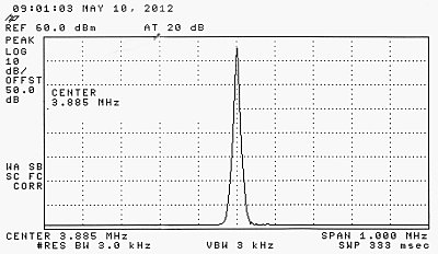
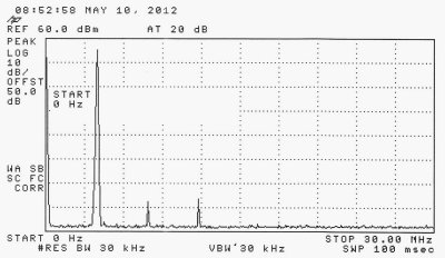
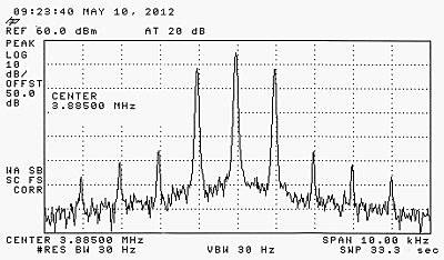
This is a look at the transmitter modulated by a single 1000 Hz tone. Total harmonic distortion is on the order of a few percent.

triangle waveform

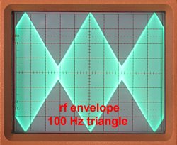
Results of the 100 Hz triangle test. Additional tests were run using sine, square and triangle waves throughout the transmitter audio passband with excellent results.

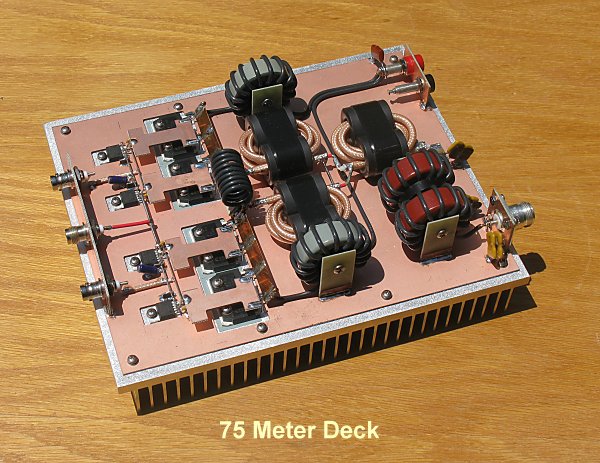
Construction Details

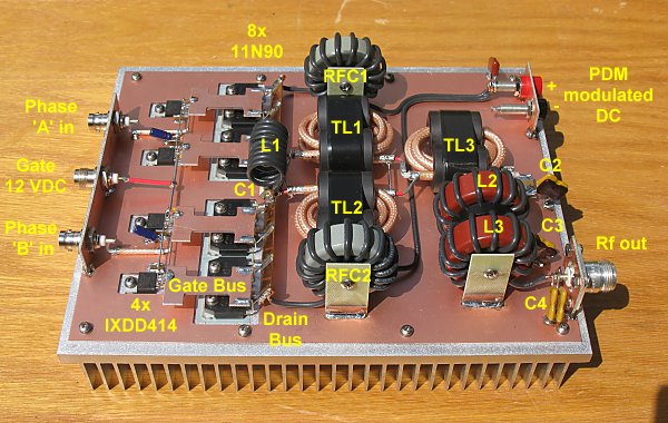
Any number of different layouts and construction techniques could likely be used for the CMCD decks, however those shown here have been proven to work. Keep in mind that lead lengths should be kept as short as possible to minimize stray inductance. To this end, mount the drivers ICs close to the FETs and use wide conductors to make the connection. Driver IC ground and FET source pins should be as short as possible. FETs should be mounted as close together as the Silpad insulators permit. This will minimize the width (inductance) of the drain bus. Keep the input/output connections of the transmission line transformers as short as possible. Driver IC 12 volt 'rails' require reasonably heavy gauge wire and should be well bypassed.

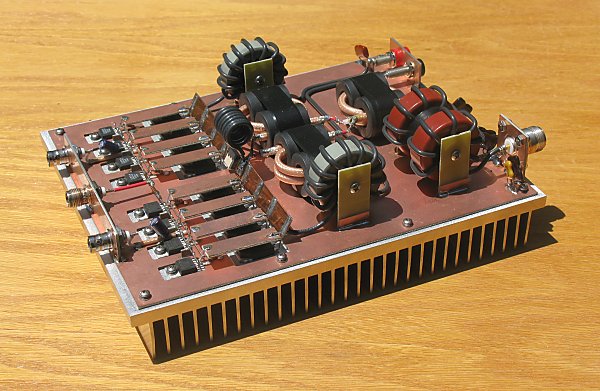
The picture below shows the layout.

Parts Placement

All three decks are built on 8" X 10" X 1-1/4" aluminum heatsinks. Double sided .062" glass epoxy circuit board milled out for the drivers and FETs is attached to the heat sink and provides an excellent ground plane. Drivers ICs bolt directly to the heatsink and the FETs are insulated with Silpad insulators. Additional pieces of circuit board material are used to support the input and output connectors, banana jacks and as supports for the rf chokes and low pass filter inductors. Delrin rod is used as spacers between the circuit board pieces to support the cores. An additional 1/4" delrin 'washer' is used between the two low pass filter inductors to keep them separated. Eventually these decks will be enclosed in rf tight enclosures although there have been no issues operating them in the open.

Most of the construction is fairly obvious but a few things are worth mentioning.

A low impedance driver 12 VDC rail is important because of the high gate capacitance charging current. #16 (or larger) wire should be used and each driver IC should have it's own 0.1 uF ceramic bypass. Large chip caps (1825 size) were used here. Leaded capacitors would also work as long as the leads are kept short. Each rail has it's own electrolytic capacitor.

Driver IC's are connected to the FETs with 3/8" wide conductors. The dogbone shaped pieces of circuit board used here were left over from another project. A single driver IC is capable of driving two FETs on 160 and 75 meters. On 40 meters one driver IC is required for each FET.

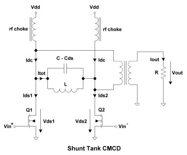
The drain buses are made from 1/2" wide copper flashing. C1, the shunt resonator capacitor, is an ATC 100E series capacitor (or two units in series or parallel - see schematic for details) with stripline leads that solder directly to the "A" and "B" phase drain buses. L1, the shunt resonator inductor is soldered to the drain buses on each side of C1.

TL1 and TL2 form the 4:1 transmission line transformer. Each half is wound on two sleeve cores that are taped or epoxied together. As noted on the schematics these are wound with 25 ohm coaxial cable. Only miniature sized 25 ohm coax is readily available so one must construct their own. This is easily done by removing the existing center conductor and insulator from RG-303, RG-142 or RG-400 and replacing it with insulated #14. Stranded wire is best as the winding radius is somewhat tight.

For clarity, the winding count is given as 'passes' instead of turns. A pass is defined as the coax passing through either core. The 5 pass windings fit easily on the cores. The 7 pass windings are a bit of a tight fit.
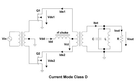

Operation

The CMCD decks have no tuning and loading controls - only a low pass filter to remove harmonics. This means that the transmitter requires a load fairly close to 50 ohms so that the FETs see the proper drain impedance via the output transformer. Some VSWR (~ 1.5:1) is tolerable and will be seen as a shift in the drain voltage/current ratio. If one normally uses an antenna tuner, this is less of an inconvenience since the load will be close to 50 ohms. In effect, the antenna tuner takes the place of a conventional amplifier tuning and loading controls.

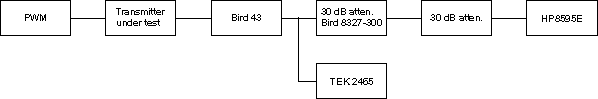
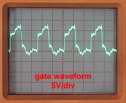
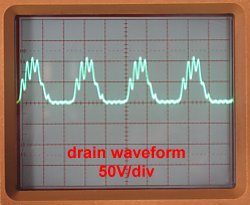
When first powering up the CMCD decks, the shunt tank (C1/L1) should be adjusted for resonance at the center of the band in use. Set the VFO or other signal source to the center of the band and key the transmitter at reduced power (~100 watts output) and spread or compress the turns of L1 for minimum drain current. If a scope is available, verify the drain waveform looks similar to that shown above.

The table below shows the typical operation at the 375 watt carrier level.


Band

Gate V/I Drain V/I Input Power Output Power Efficiency
 
160 Meters 12.0V/1.5A 36V/11.1A 400W 370W* 92.5%*
 
  75 Meters 12.0V/3.3A 35.9V/11.A 400W 370W* 92.5%*
 
  40 Meters 12.0V/6.0A 35.8V/11.2A 400W 365W* 91%*


* These are approximate values. While it's possible to accurately measure the dc voltage and current input of the transmitter using digital meters, measuring the rf power to the degree of accuracy required for these efficiency levels is much more difficult. Bird 43 wattmeters are usually much better than their 5% FS stated accuracy spec but consider that a 10 watt error (less than half of the rated 5% FS accuracy) results in a 2.5% efficiency uncertainty. Another source of error is the Bird 8327-300 power attenuator, which are known to drift slightly in impedance and attenuation. A more accurate way to measure rf power is being investigated and the numbers presented here will be updated as better measurements are available.

Note the Gate V/I (power) in the table above. This is the power required to drive the gates of the FETS. 160 meters requires 18 watts, 75 meters requires 40 watts and 40 meters requires a whopping 72 watts! This power is dissipated as heat. It's interesting to note that drain dissipation at 92% efficiency is only about 30 watts. As expected, in operation the 40 meter deck gets noticeably warmer. These decks are capable of carrier power beyond 375 watts. Limited testing has been performed at 40 volts/12.5 amps.

Photo below of the 40 meter deck ... same design and layout but with 4 additional driver ICs.

40 Meter Deck

Back to W1VD / WD2XNS home page