|
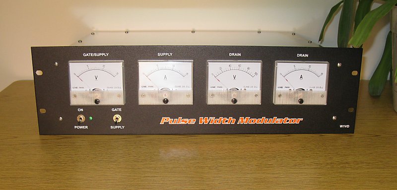
The high efficiency Pulse Width Modulator shown here was designed for use with homebrew current-mode, Class-D amplifiers for 160, 80 and 40 meters described elsewhere on this website. It can also be used with other classes of amplifiers such as the popular Class E rigs as the requirements for a modulated dc supply are the same. The modulator as shown is configured to power legal limit (375 watt carrier) transmitters at >150% modulation ... with power to spare.
Theory of Pulse Width Modulators, as well as Class E transmitters, is covered in detail on the Class E website and is recommended reading. In fact, the three PWM related circuit boards in this modulator were obtained from Steve, WA1QIX, proprietor of Radio Engineering Associates (REA) and 'keeper' of the Class E website. These are high quality boards that greatly simplify the PWM building process and are reasonably priced so there is little reason to 'roll your own'. A number of PWM modulators have been constructed using the REA boards and they share similarities but also differ as the builder customizes them to fit the station requirements. Some features of this modulator are outlined below.
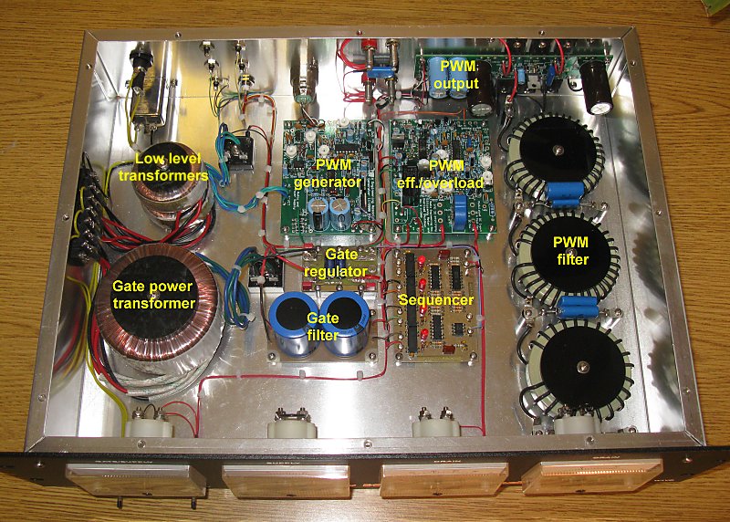
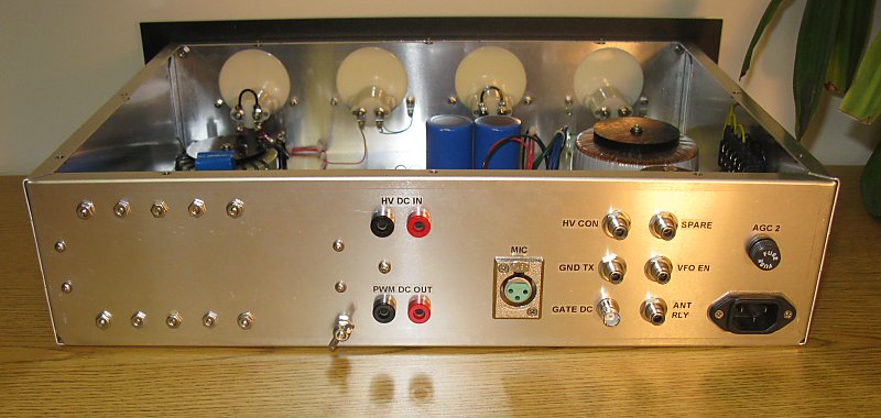
The enclosure makes use of commercially available components - a 3ru (5.25") high aluminum rack panel and a 13" X 17" X 4" aluminum chassis used 'upside down' to house the various components. The main components are noted in the the picture below:
|
|
The PWM boards are covered in detail on the Class E website so we'll stick to what's different about this modulator. Since the Class D decks use digital gate drive a moderatly high current 12-volt, dc power supply is included. To drive the transmitter's eight FET gates requires roughly 1.5 amps on 160 meters, 3 amps on 80 meters and 6 amps on 40 meters. The gate supply used here can deliver in excess of 8 amps. It consists of an Antek 22 volt/200 VA toroid transformer, full wave rectifier module, filter and a high efficiency (85%+) Vicor dc-dc converter. Model number V24C12T100BN was used here and operates with an input range of 18 - 36 VDC and outputs 12 VDC at 100 watts. These modules utilize zero voltage, zero current switching circuitry and have low noise (< 200 mV), excellent load regulation (.02%), over/under voltage shutdown as well as over current protection. While somewhat expensive when purchased new, they can be had for reasonable money, like this one, on ebay. A .pdf datasheet on this series of regulators can be found here. The circuit board mounted to the top of the module facilitates interconnection. The 28 volt input to the regulator also powers the T/R relay - a high isolation 'mil' type that has a 28 volt coil and the 12 volt ouput powers the VFO and sequencer module. Two transformers for the PWM generator/output/overload board +12 vdc, +5 vdc and - 12 vdc requirements are also Antek toroid types - 15 volt/50 VA. These are stacked vertically.
Also shown is a comercially available sequencer board. This board provides sequential outputs 30 msec apart and is used to control the receive-to-transmit and transmit-to-receive transition to prevent 'hot switching' and other anomolies. Grounding the sequencer input initiates the receive-to-transmit transition and the sequence goes like this: 1) antenna relay is switched from receive to transmit; 2) VFO operation is enabled; 3) the efficiency/overload board reset is asserted. At this point the efficiency/overload board relays are activated and simultaneously apply the transmitter's gate 12VDC and activate the HV contactor. If an overload situation occurs the efficiciency/overload board detects the problem and shuts down the gate 12 VDC and the HV. The sequencer remains keyed (until it's input is released from ground) but the efficiency/overload board has stepped in and done it's job - protecting the amplifier FETs. Releasing the sequencer input from ground completes the cycle in reverse order as follows: 1) the efficiency /overload board reset is released; 2) VFO is disabled; 3) antenna relay is switched from transmit to receive. This may seem a bit complicated but orderly transitions can save components from premature failure.
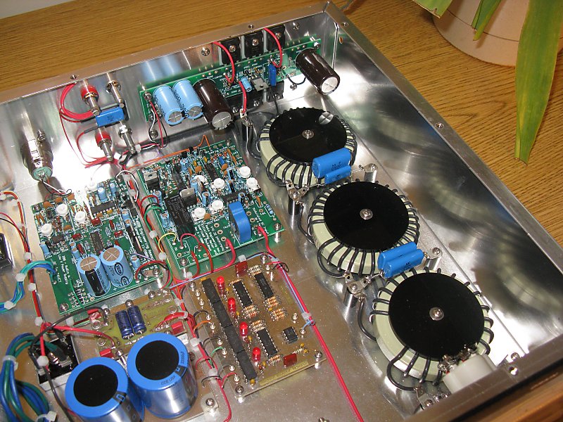
The 6 element PWM output filter uses three high flux CH77060/C058867A2 cores. Single cores, as used here, are suitable for power levels up to about 500 watt carrier. Beyond that, cores must be stacked or multiple coils used in parallel to handle the high dc and ripple currents - especially for the first coil in the filter. As one approaches the 1 kW carrier level conventional air wound coils make more sense as the amount of core material required to support the high flux becomes unmanageable. The filter used here is an 'infinite impedance' Butterworth design which, in Spice simulation, provides better transient response than other filter designs. Whether or not this is descernable over the air has yet to be determined.
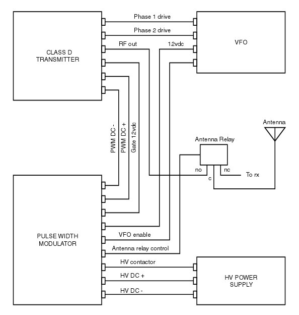
The transmitter system is 'modular' with four sections or 'modules': 1) Class D RF amplifier; 2) VFO; 3) Pulse width modulator; and 4) HV power supply. When designing the modulator it was determined that this module would house most of the circuitry that controls or powers other modules - therefore it has a number of interconnections on the rear panel. A drawing of wiring layout is shown below.
|
|
The picture below show more detail on the construction. The PWM output board was populated with three FETs and diodes and mounted to the rear panel in case a heatsink was required for cool operation of the FETs. Efficiency turned out to be so good that in ICAS the chassis is a sufficient heat sink. It would be a simple matter to add a vertical mount heat sink if desired.
Delrin mounts were machined to hold the PWM filter toroid cores off the chassis and delrin standoffs support solder lugs that provide tie points for the filter connections. Because of the high currents involved, and limited screw torque that can be applied for delrin, the three lugs are soldered together. The ground end of the filter capacitors are attached to solderlugs on aluminum standoffs. This makes it convenient to swap out PWM filter components if experimenting with other filter types.
|