|
This 137 & 500 kHz Class-D Kilowatt rf deck was built for use at WD2XNS (136 - 138 kHz) and WE2XGR/2 (465 - 515 kHz) to transmit modes that don't require linear amplification - cw, QRSS and various FSK modes. Transmissions that require linear amplification are handled by a linear phasing exciter and Hafler 9505 power amplifier - details are elsewhere on this website.
Circuit Details
This rf deck is a simplification of an earlier kilowatt setup that combined two 500-watt decks to generate the kilowatt power level. While that setup worked well and had the ability to remain on the air at reduced output if one module failed, the decks proved so reliable that a redundant system with its additional complexity was deemed unnecessary. The two rf decks and combiner have been replaced by a simplified 'all-in-one' kilowatt deck. The original 'modular' design concept is followed here with the the low-pass filter as a separate module.
The schematic diagram of the 137 and 500 kHz kilowatt decks can be found at
137 & 500 kHz Kilowatt Deck .
Since the kilowatt deck development was essentially a 'build out' based on the earlier 500-watt deck a number of comparisons will be made. Information on the original 500-watt decks can be found at
137 & 500 kHz Kilowatt Transmitter
Comparing the 500-watt deck to kilowatt deck shows a great degree of similarity. Both are Voltage-Mode Class D (VMCD) topology with the kilowatt version using twice the number of FETs. Changes to the earlier driver circuit were made to accomodate the additional FETs as well as provide a few other improvements; keying from either a '- key' (standard keyer) or '+ key' (RS-232), cw keying the IR2110 S/D (shutdown pin) for better gate waveform control and providing an input to the IR2110 S/D from an overload shutdown circuit (currently in use and soon to be documented).
The four FETs (two each phase) are driven by the IR2110 through 10 ohm/1N4148 diodes that slow gate turn on and speed up gate turn off. This provides additional off time between the phase transitions and helps prevent cross conduction as well as providing some isolation between the two gates. The IR2110 drives the pairs of gates easily on 137 kHz but with some temperature rise on 500 kHz. For this reason, swapping in FETs with significantly higher gate capacitance should be avoided.
LTSpice simulation indicated the need for a choke between the centertap of the transformer and Vcc and that the electrolytic bypass capacitor be increased in value to control ripple at the higher operating current. Simulation also demonstrated the significant current spikes in the transformer center tap bypass capacitor. A number of capacitor types would likely survive in this application but I chose to parallel 0.1 uF chip capacitors (1825 size) that were on hand. The 'stacked' chip caps run cool to the touch. Other capacitor types should be checked for temperature rise as indication of their suitability.
At the kilowatt level issues developed with the output transformer. The FT-240-77 cores that worked well in the 500-watt deck began to show signs of 'stress' while testing the prototype 137 kHz kilowatt deck. The core ran noticeably warm to the touch, transition ringing on the drain waveform was difficult to tame and efficiency was less than expected. Additional core losses at the increased power level and excessive leakage reactance were to blame. After a study of the ferrite literature, the best solution appeared to be a switch to 78 ferrite material which was designed specifically for the 100 - 200 kHz frequency range. As luck would have it, 78 cores were available in FT-240 size and readily available through several distributors! A few days later FT-240-78 cores were being tested in the prototype 137 kHz deck. The cores just warm to the touch, ringing was much easier to tame and efficiency was back in the mid 90% range.
During development of the prototype 500 kHz kilowatt deck it was clear there was no point in even trying 77 material at the higher frequency as losses would only be worse. An output transformer was wound on the 'new' 78 material core. This worked well but at noticeably higher temperatures than at 137 kHz. Drain ringing at the transitions was well controlled and efficiency was almost as good as at 137 kHz. The core temperature rise was well within allowable limits so that could have been the end of the story ... but looking through the ferrite information I noticed 79 material. This material had excellent specs up through 750 kHz but the material was so new there were only two different core sizes available - neither suitable for this project. After some 'mental handwringing' it was decided to pay the NRE charge to have a number of FT-240-79 cores built. Several months later the cores arrived and, as expected, they work very extremely well. Performance was on par with 78 material at 137 kHz. It was hoped that Fair-rite would add this and other 79 material cores to their catalog but at last check there are none listed.
So then the obvious question is what core material to use at 500 kHz? If you're building this deck to run a very conservatively rated half kW output then the 78 material is fine. If you are building this deck to run the full kW output key down for prolonged periods of time then 79 material might be a better choice. Anyone seriously considering building this deck can check with me on core availability.
Construction Details
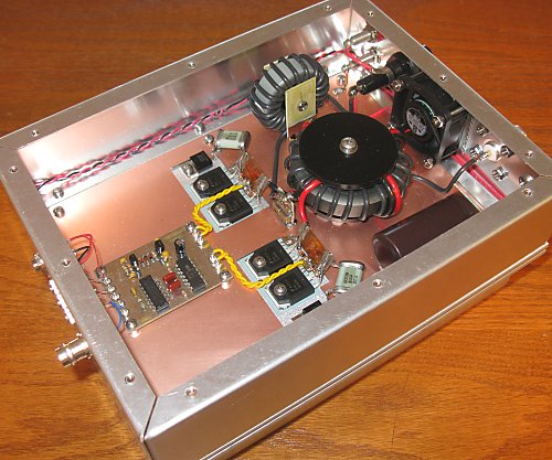
A construction technique similar to the 500-watt decks was used for the kilowatt deck. Many of the details can be seen in the following pictures.
|
|
|
|
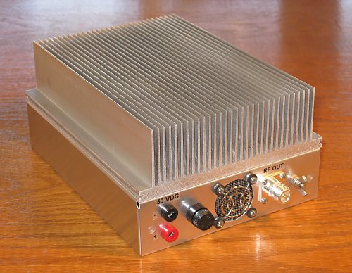
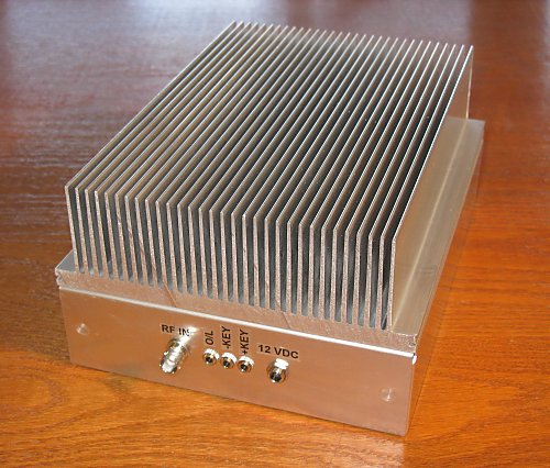
The housing is constructed using a standard sized chassis mounted to a heatsink. A Bud AC-406 7" X 9" X 2" inch aluminum chassis has the top side cut out to the same dimesions as the bottom. Input and output jacks, fuse holder, fan, etc. are mounted to the chassis which in turn is attached to the heatsink. Double sided circuit board is fit into the chassis cut out and forms the ground plane for various connections and mounting of components. Two areas of the circuit board have been milled out so that the FETs and snubber resistors can mount directly to the heatsink. The heatsink is drilled and tapped for 4-40 screws that are used to mount the FETs, snubber resistors and the chassis to the heatsink.
The heat sink is a standard extrusion from Antek and is 7" in width - same as the width of the chassis. Antek will cut the heatsink to a length of 9" (part number HS0709) so it is exactly the size required to mount to the chassis. Fin height is 2" which is overkill for the amount of power that needs to be disipated - even when key down for long periods. The choice of heatsink was a practical matter as there are very few reasonably priced (less than $25 for this one) off-the-shelf extrusions available in just the right size. Key down periods of 15 minutes at the kilowatt output level barely raise the heatsink temperature above ambient.
All of the driver components are mounted on a printed circuit board. Short leads connect the circuit board to the rf input, power, overload and keyer jacks. #20 stranded teflon wire is used for the twisted pairs that connect the output of the board to the FETs. Silpads insulate the FETs from the heatsink. The T0-220 thick film snubber resistors mount directly to the heatsink with no insulators.
|
|
|
|
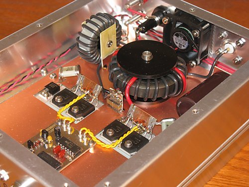
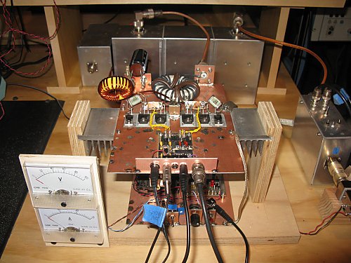
The output transformer is constructed as follows. The first winding placed on the core is the #14 solid copper THHN seconday. These turns are equally spaced around the core. The #12 bifilar primary winding is made from two #12 stranded THHN wires that are held tight together with clear heat shrink tubing. This winding is wound over the secondary and also spaced equally around the core. To minimze leakage reactance the primary and secondary must be in close contact with each other. To this end the core and windings are sandwiched between two 1/8" delrin washers along with a center delrin spacer. The delrin washers and center spacer secure the windings and provide insulation from the copper ground plane. An 8-32 stainless machine screw secures the assembly to the heatsink.
The pairs of FET drains are connected together with 3/8" wide pieces of copper flashing to minimize inductance. The output transformer primary leads are soldered to the copper flashing as are the snubber capacitor leads. The 10 ohm / 1N4148 gate components are soldered directly to each gate lead and connect to the gate drive twisted pair wires.
The rf choke is supported by two 3/4" wide X 1-1/2" long pieces of circuit board material that are soldered to the ground plane. The copper cladding was removed from all but the bottom 3/8" of the pieces. A threaded delrin spacer supports the coil in position.
The 4700 uF electrolytic capacitor is mounted to a 1" X 1" piece of circuit board that is also soldered to the ground plane. This can be seen to the right of the output transformer. A small strip of copper cladding was removed from between the two capacitor terminals.
In similar fashion, the individual 0.1 uF chip caps that form the transformer center tap bypass are soldered to a 1/2" X 3/4" piece of circuit board material. Capacitors are 'stacked' in two rows of three and soldered to the circuit board, which in turn is soldered to the ground plane. This technique makes for a very low inductance capacitor.
Since this deck will experience long periods of key down transmissions at full output power a miniature muffin fan was included to move small amounts of air over the transformer. The 24 VDC, 40 cm X 40 cm X 20 cm muffin fan is run on 12VDC. This provides just the right amount of air flow and almost no noise. The chassis bottom cover is made from performated aluminum which allows the forced air to escape with little backpressure ... as long as rubber feet are used to support the amplifier bottom above the operating surface. Tiny rubber washers were used on the fan's mounting screws to isolate mechanical vibration. Coarse stainless steel screening between the fan and chassis maintains the rf shielding.
Low pass filters for 137 and 500 kHz used after the kilowatt deck have been previously described and can be found at LF and MF Kilowatt+ Low Pass Filters. "T" type low pass filters (not pi type) must be used with Voltage Mode Class D (VMCD) transmitters.
Spectral Analysis
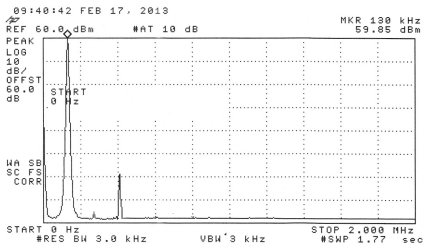
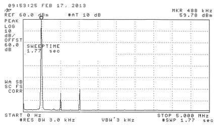
For the following spectral analysis the decks were run at a nominal 50 VDC / 20 A resulting in 1 kW input. Output power for each deck is roughly 950 watts - efficiencies are in the mid 90's.
|
|
|
|
The spectral display above shows the output of 137 kHz deck with low-pass filter. The top line of the graticule is +60 dBm (1 kW) and the vertical display is 10 dB per division.
|
|
|
|
The spectral display above shows the output of the 500 kHz deck with low-pass filter. The top line of the graticule is +60 dBm (1 kW) and the vertical display is 10 dB per division.
Additional Notes
The power supply used for this deck is about as simple as it gets. A dual output Antek toroidal power transformer (AN-15440) feeds separate full wave rectifier bridges and capacitor banks. The two 'separate' power supplies are combined at the back of the deck allowing the use smaller (#14) gauge wire. Unregulated supplies are more efficient than regulated supplies and as long as the capacitor bank is sufficiently large the CW note is clean.
The primary of the power transformer is fed through a large Powerstat thereby controlling the output DC voltage. By adjusting the DC voltage over the 0 - 50 VDC range the deck will produce any power level from 0 - 1000 watts output. No adjustment other than the Powerstat is required and efficiency remains very close to optimum across the entire power range.
This deck is used in conjunction with an overload shutdown system (writeup coming soon). The system senses an overload condition, either high current and/or high VSWR (both levels setable), and initiates a shutdown. Within a few microseconds, the pulse train to the FET gates is shut down via the IR2110 S/D feature thus turning off the FET drain source channels. At the same time the contactor in line with the FET drain supply opens to remove VDC from the deck. Because of the contactors physical size this takes 10's of milliseconds - several order of magnitude too slow to protect the FETs from damage but fast enough to prevent other damage including protecting the fuse. The system has been in use for over a year now and has shown it's ability to protect the decks from just about any mishap. The overcurrent level is adjustable and can be set for any power level and associated current draw.
It might be possible to make a single deck that covers both 137 and 500 kHz with no component changes. This would require a few compromises but may be a possibility. As time permits I'll be looking into this. In the overall scheme of things, though, the price of building two optimized decks, one for each band, is not cost prohibitive.
I always like to include a picture of the prototype that came before the finished product. This picture of the
prototype 137 kHz deck shows the rather ugly construction details. The overload shutdown board is mounted on the lower level of the test fixture. Prototypes are alot more fun than the finished product as almost 'anything goes' construction wise while exploring all of the 'what ifs'. This deck was operated for well over a year just as seen in the photo - unshielded and out in the open. No interference problems were noted.
|
|
Back to W1VD WD2XNS WE2XGR/2 home page
|
|
| | | | |